Optica Vol. 11, Issue 1, pp. 42-47 (2024)
Matan Iluz, Kobi Cohen, Jacob Kheireddine, Yoav Hazan, Amir Rosenthal, Shai Tsesses, and Guy Bartal
Abstract:
Silicon photonics leverages mature semiconductor technology to produce cost-effective and high-performance components for various applications in data centers, artificial intelligence, and quantum computing. While the geometry of photonic integrated circuits can be characterized by existing means, their optimal and accurate performance requires detailed characterization of the light propagating within them. Here we demonstrate the first, to our knowledge, direct visualization of the light as it travels inside photonic integrated circuits. We employ the natural nonlinear optical properties of silicon to directly map the electric field of the waves guided inside the integrated circuits, characterizing waveguides and multimode splitters while extracting various parameters of the device—all in real-time and in a noninvasive manner. Our approach for visualizing light inside photonic circuits is the only solution directly providing such information without any overhead or penalty, potentially making it a crucial component for the characterization of photonic circuitry, toward their improved design, fabrication, and optimization.

Imaging light within the MMI splitter. (a) Optical imaging of the MMI device. (b) Direct mapping of the light evolution inside an MMI device. The figure comprises exposures of seven different locations along the device, stitched together to track the evolution in the MMI. The rightmost exposure is at the single-waveguide input while the leftmost is of the two waveguides. (c) Zoom-in of (b). (d) Simulation results on a similar scale to (c). (b)–(d) show the intensity of the transverse electric field. Evidently, the experimental results are in excellent agreement with the simulation of light evolution in such a system.
.
Optica Vol. 11, Issue 1, pp. 42-47 (2024)
Matan Iluz, Kobi Cohen, Jacob Kheireddine, Yoav Hazan, Amir Rosenthal, Shai Tsesses, and Guy Bartal


 Fig. 3D optoacoustic reconstruction of a surgical suture. (a) 2D maximum amplitude projection image of the suture. (b) Photograph of the suture showing the similarity between the reconstruction and the imaged object. (a) and (b) are the same scale. (c) 2D slice along the white dashed line shown in (a); shows the cross-section of the suture and demonstrates the lateral and
 Fig. PA image of (a) water acquired by 1930-nm OR-PAM and b lipid acquired by 1750-nm OR-PAM; c Overlaid PA image of (a) and (b). d Photography of the adipose tissue. e–f Three-dimensional rendering view of (a, b). Scale bars, 500 µm


 The study was supported by the Russell Berrie Nanotechnology Institute (RBNI), the National Science Foundation, the Polak Foundation, the Israel Innovation Authority, the Israel Science Foundation and the Ollendorf Minerva Center.
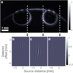
 Fig. Imaging experiments. (a),(c) Optical images of acoustic targets. (b),(d) Ultrasound images of the targets shown in panels (a),(c). (a),(b) Images of 50-µm tungsten wires. (c),(d) Images of lamb meat and fat tissue; (d) is a 1D line scan image along the dotted line shown in panel (c); on the right side are three 0.5 mm × 0.5 mm close-up images. The image in panel (d) is “rolled” and shown in the polar coordinate system.

 Fig. In-vivo Tomographic imaging. Figure 8-a: Microscope images of mouse ear (left) and corresponding MIP of the optoacoustic image (right). Figure 8-b: Montage of four different tomographic depth. The depth difference between each consecutive slice was 50 μm. Figure 8-c. Typical raw OA signals from a mouse ear. Scale bar: 1 mm

 Figure – Normalized power spectrum measured in the spatial position in which the AOI was maximal using conventional ToF-AOI with a PMT (blue) and our homodyne approach with a PD (red). A consistent decrease in noise level measured in both cases in favour of PD. The 2nd and 3rd harmonics of the US signal are visible for both techniques. (Color figure online).
 Figure-Optoacoustic images of the blood vessels in a human wrist, at different depths and orientations. A cross-section of the radial artery can be seen clearly in real time at depths up to 7 mm, as in (a,c). A deep vein can be seen in (b) at a depth of 8 mm. In (d), we can see a vein diving from 3 to 7 mm in a longitudinal cross-section. The scale bar in subfigure (a) applies to all subfigures.